Government Grants
Business Grants
Home Owner Programs
Federal Programs
About Us
Development of Large Diameter Silicon Carbide Substrate and Epitaxial Processes
This is a sources-sought synopsis in the area of:
Gallium Nitride (GaN) High Electron Mobility Transistors (HEMTs) are rapidly becoming the technology of choice for high power RF applications.
GaN RF devices are dependent upon the use of high quality, semi-insulating SiC substrates.
/>
The combination of high voltage and current handling as well as switching frequency capabilities make SiC based power devices a viable alternative to silicon technology.
Fabrication of SiC power devices requires homo-epitaxial growth of precisely doped SiC layers ranging in thickness from a few microns to > 100 μm depending upon the voltage requirements.
Critical to the realization is the availability of affordable, high quality, large diameter SiC substrates and epitaxy from a pure play supplier.
The Air Force Research Laboratory (AFRL) is interested in advancing the current technological state-of-the-art with respect to SiC growth and fabrication.
Agency: Department of Defense
Office: Air Force -- Research Lab
Estimated Funding: $13,500,000
Office: Air Force -- Research Lab
Estimated Funding: $13,500,000
Who's Eligible
Obtain Full Opportunity Text:
Not Available
Additional Information of Eligibility:
Not Available
Full Opportunity Web Address:
Contact:
Jo Ann SillamanGrants Officer/Contracting OfficerPhone 937-713-9965
Agency Email Description:
For Questions & Assistance
Agency Email:
jo.sillaman@us.af.mil
Date Posted:
2016-03-18
Application Due Date:
2016-04-18
Archive Date:
2016-05-18
Follow @topgovtgrant
Social Entrepreneurship
Spotlight
Social Enterprise Version 2.0

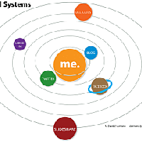
Midsize businesses are tapping into the social business market because large companies do not need the help of start-ups to create a “social technology stack.” But a social business stack cannot generate revenue by itself.
Nonprofit Jobs in Alabama
Fundraising & Development Jobs
Social Services Employment
Substance Abuse Jobs
Program Director Jobs
Social Services Jobs


